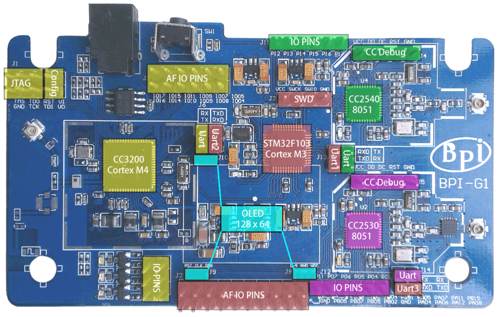
What’s BPi-G1
BPI-G1 is an integrated IEEE802.11 b / g / n (WIFI wireless network), IEEE802.15.4 (Zigbee), IEEE 802.11-2007 Standard (Bluetooth Low Energy4.0) development board. It is very easy to put these wireless protocol seamlessly together, you can exchange any different transport protocols, and three kinds of wireless protocols are integrated by three single-chip SOC, you can easily create your own Internet of things (IoT). WIFI part of which is the use of TI’s CC3200, which is a high-performance ARM® Cortex®-M4 wireless SOC, internally integrated TCP / IP protocol stack, simply use the BSD Socket can connect to the Internet. The Zigbee is used TI CC2530, which integrates wireless capabilities and enhanced 8051 core SOC, TI after years of improvement, it is already quite mature and stable, TI’s Z-stack has achieved Zigbee 2007 / Pro, you can use the 16’s short address, you can use the 64-bit long address communication, face large local interconnect systems, advanced security encryption and mesh network structure can easily cope. Bluetooth 4.0 (BLE) using TI CC2540 / 1, an integrated BLE stack and enhanced 8051 core, low-power wireless SOC, at present, most mobile phones have support for Bluetooth 4.0, both as a wearable device, or mobile interactive Accessories, CC2540 can be easily completed. Meanwhile BPI G1 also incorporates a high-performance STM32 ARM® Cortex®-M3 microcontroller, which will help you deal with time-consuming data or transit, the three wireless SOC coordinated. Therefore, the use of BPI G1 can help you quickly achieve a variety of things DIY design.
Hardware Specifications
| Items | Hardware Specifications |
| CPU | STM32F103CB ARM Cortex™-M3 32-bit RISC core |
|
WIFI |
CC3200 device is an integrated high-performance ARM Cortex-M4 MCU and with a Wi-Fi network processor subsystem (This subsystem includes 802.11 b / g / n radio, baseband, network protocol stack and a powerful encryption engine MAC, supports 256-bit encryption in order to achieve a fast, secure Internet connection). This device contains a variety of peripherals, I2S, SD / MMC, UART, SPI, I2C and four-channel analog to digital converter (ADC). |
| Bluetooth |
CC2540 device is a low cost, low power, true system-on-chip (SoC) for Bluetooth low energy applications. It enables to build a strong BLE master or slave node with very low total cost BOM. The CC2540 combines the excellent RF transceiver, the industry-standard enhanced 8051 MCU, in-system programmable flash memory, 8 KB RAM and many other powerful auxiliary functions and peripherals. |
| Zigbee |
CC2530 device is a true system-on-chip (SoC) for IEEE802.15.4, Zigbee RF4CE applications and solutions. It enables the establishment of a strong network of nodes and very low total cost BOM. CC2530 combines leading RF transceiver, the industry-standard enhanced 8051 MCU, in-system programmable flash memory, 8 KB RAM outstanding performance and many other powerful features. |
| Power | 5V DC |
| Buttons | Reset button |
| LED | WiFi Bluetooth Zigbee |
| Monitor | OLED(128×64) |
|
OS |
Free-RTOS、Ti-OS、Coustom-OS |
| Size | 95*56mm |
| Weight | 19g |
What can I do with BPI-G1?
1.Smart Home.
2.Intelligent Gateway
3.DIY electronic control
1.2 Main features
• Multi-module integration, development board does not occupy a small space
• Multi-protocol integration, to meet the Internet of things needs of various wireless connections
• Rich interface, no matter which one you want to achieve functional modules can easily match
• Abundant development resources, open source sharing of data and TI, ST and other major manufacturers improve the development of information
• IOS and Android devices open software interface helps you quickly connect a handheld control device
• Zigbee wireless integrated power amplifier section, an open area can reach as far as 3 km of intercellular communication
1.2 Which IDE development can use?
TI CC3200:
Code Composer Studio (CCS)
IAR EWARM
GCC
TI CC2530/CC2540:
IAR EW8051
Instant Contiki
STM32F103CB:
IAR EWARM
GCC
1.3 Which emulator debugging?
TI C3200:
BPI OpenDebugger
TI CC2530/CC2540:
BPI OpenDebugger
TI CC Debugger
TI SmartRF04EB
TI SmartRF05EB
STM32F103CB:
BPI OpenDebugger
JLink V8
STLink V2
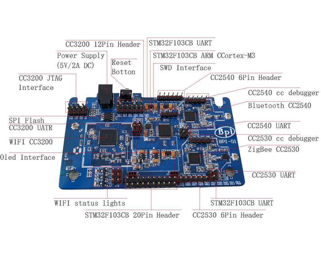
2 Hardware Description
2.1 Some of the features TI CC3200
• ARM Cortex-M4 core, 80MHz operating frequency
• Embedded memory RAM (up to 256KB)
• External serial flash boot loader, and the ROM peripheral drivers
• 32-channel direct memory access (DMA)
• For advanced fast security hardware encryption engine, including
AES,DES and 3DES
SHA2 and MD5
Cyclic Redundancy Check (CRC) checksum
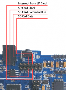
• 1 SD / MMC interface
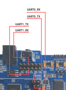
• 2 Universal Asynchronous Receiver Transmitter (UART)
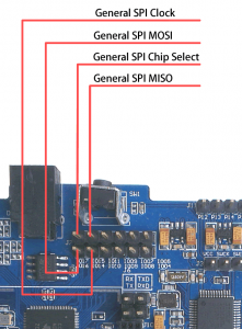
• 1 serial peripheral interface (SPI)
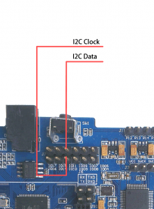
• 1 inter-integrated circuit (I2C)
• 4 general-purpose timers, support for 16-bit pulse width modulation (PWM) mode
• 1 watchdog timer
• 4-channel 12-bit ADC (ADC)
• Up to 12 independently programmable, reusable general purpose input output (GPIO) pins
• Built-in TCP / IP stack
Industry standard BSD socket application programming interface (API)
8 simultaneous TCP sockets or UCP
2 slots while TLS and SSL
• Strong encryption engine for the 256 for AES TLS and SSL encrypted connections fast, secure Wi-Fi and internet connection
• Base stations, access points (AP) and Wi-Fi Direct Mode
• WPA2 Personal and Enterprise Security
• For independent and fast Wi-Fi connection SimpleLink Connection Manager
• SmartConfig technology, AP mode and WPS2, these techniques used to implement a simple and flexible Wi-Fi hotspot
• Tx power
18.0 dBm @ 1 DSSS
14.5 dBm @ 54 OFDM
• RX Sensitivity
-95.7 dBm @ 1 DSSS
-74.0 dBm @ 54 OFDM
• Advanced low power mode
Support real-time clock (RTC) Sleep: 4μA
Low power deep sleep (LPDS): 120 μA
RX flow (MCU activation): 59 mA @ 54 orthogonal frequency division multiplexing (OFDM),
TX flow (MCU activation): 229 mA @ 54OFDM, maximum power
Idle connections (in LPDS in MCU): 695 μA @ DTIM = 1
• Clock Source
40.0MHz crystal with internal oscillator
RTC 32.768kHz crystal or external clock
2.2 Some of the features TI CC2530
• Excellent performance and low power 8051 microcontroller core with code prefetch feature
• 256K system programmable flash memory
• 8KB RAM, with a power supply in a variety of data retention
• Hardware debugging support
• The powerful 5-channel DMA
• Integrated high-performance operational amplifiers and ultra low-power comparator
• IEEE 802.15.4 MAC timer, general-purpose timers (one 16 bit, two 8 bit)
• IR generating circuit
• 32-kHz sleep timer capture
• CSMA / CA hardware support
• Accurate digital RSSI / LQI support
• 6 channels can be configured 12-bit ADC resolution
• AES security coprocessor
• 2 Powerful USART interface to support multiple serial protocol
• 1 common SPI interface
• 8 general purpose I / O pins (6 × 4 mA, 2 × 20 mA)
• Watchdog Timer
• Wireless Performance
Adapt 2.4GHz IEEE802.15.4 RF transceiver
High receiver sensitivity and robustness
Programmable output power up to 4.5dBm
• Low power consumption
Active mode RX (CPU idle): 29mA
TX Active mode in 1dBm (CPU idle): 29mA
Power mode 1 (4us wake): 0.2mA
Power Mode 2 (Sleep timer runs): 0.2mA
Power Mode 3 (external interrupts): 0.4uA
Wide supply voltage range (2V-3.6V)
2.3 Some of the features TI CC2540/1
• Excellent performance and low power 8051 microcontroller core with code prefetch feature
• 256K system programmable flash memory
• 8KB RAM, with a power supply in a variety of data retention
• Hardware debugging support
• The powerful 5-channel DMA
• Extended baseband automation, including automatic recognition and address decoding
• General-purpose timers (one 16bit, two 8bit)
• IR generating circuit
• 32-kHz sleep timer capture
• Accurate digital RSSI / LQI support
• 2 channels can be configured 12-bit ADC resolution
• AES security coprocessor
• 2 Powerful USART interface to support multiple serial protocol
• 1 common SPI interface
• 8 general purpose I / O pins (6 × 4 mA, 2 × 20 mA)
• Watchdog Timer
• Wireless Performance
Suitable excellent receiver sensitivity (at 1 Mbps is -94 dBm), selectable, and barrier properties
Programmable output power up to 4dBm (2540) / 0dBm (2541)
• 2541 Low Power
RX mode low: 17.9 mA
Mode TX (0 dBm): 18.2 mA
Power mode 1 (4-μs wake): 270 μA
Power Mode 2 (Sleep timer open): 1 μA
Power Mode 3 (external interrupts): 0.5 μA
Wide supply voltage range (2 V-3.6 V)
• 2540 Low Power
RX mode low: 19.6 mA
Mode TX (-6 dBm): 24 mA
Power mode 1 (3-μs wake): 235 μA
Power Mode 2 (Sleep timer Open): 0.9 μA
Power Mode 3 (external interrupts): 0.4 μA
Wide supply voltage range (2 V-3.6 V)
2.4 Some of the features STM32F103CB
• ARM Cortex-M3 core running at 72MHz
• 128K system programmable flash memory
• 20KB RAM
• 2 × 12 bits 1 microsecond A / D converter (up to 16 channels)
Conversion range: 0~3.6 V
Dual sample and hold function
• DMA
7-channel DMA controller
Supported peripherals: timers, ADC, SPI’s, I2C and USART
• 18 general-purpose programmable GPIO
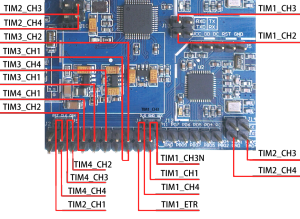
• 7 Timer
3 16-bit timers, each up to 4 IC / OC / PWM or pulse counter quadrature (incremental) encoder into
16-bit motor control PWM timer, dead-time generation and emergency stop
2 watchdog timers (Independent and windows)
System Timer: 24 downcounter
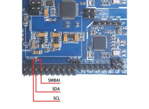
• 1 I2C interface (SMBus / PMBus)
• 3 USART (ISO7816 interface, LIN, infrared capabilities, modem control)
• 1 SPI interface (18 Mbit / s)
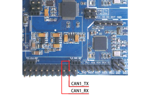
• 1 CAN interface (2.0B Active)
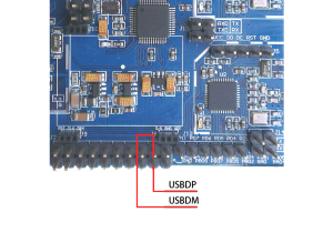
• 1 full-speed USB 2.0 interface
3 Peripheral Interface
3.1 TI CC3200 part Peripheral Interface
3.1.1 4-wire SDIO Interface
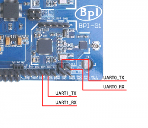
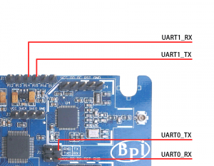
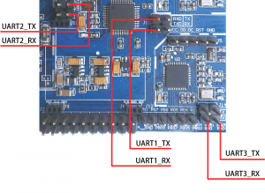
3.1.2 Uart Interface
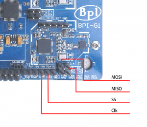
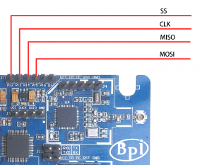
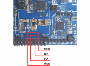
3.1.3 SPI Interface
3.1.4 I2C Interface
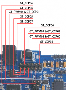
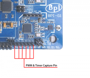
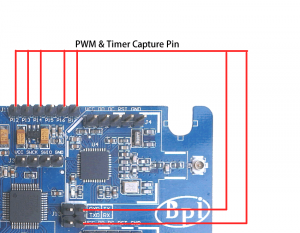
3.1.5 PWM & Timer Capture channel
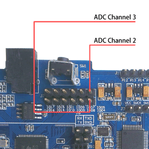
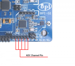
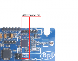
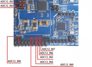
3.16 ADC channel
3.2 TI CC2530 part Peripheral Interface
3.2.1 Uart Interface
3.2.2 SPI Interface
3.2.3 PWM & Timer Capture channel
3.2.4 ADC channel
3.3 TI CC2540/1 part Peripheral Interface
3.3.1 Uart Interface
3.3.2 SPI Interface
3.3.3 ADC channel
3.3.4 PWM & Timer Capture channel
3.4 STM32F103CB part Peripheral Interface
3.4.1 Uart Interface
3.4.2 SPI Interface
3.4.3 I2C Interface
3.4.4 CAN Interface
3.4.5 USB2.0 Interface
3.4.6 PWM & Timer Capture channel
3.4.7 ADC channel
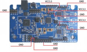
4. Global Power and Ground
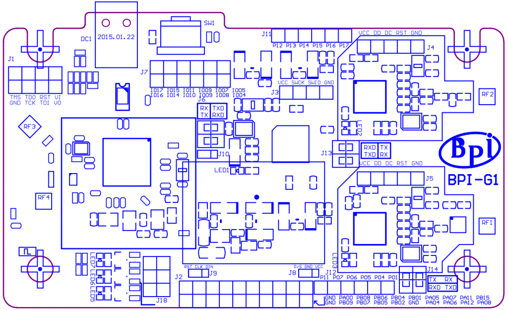
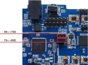
5. Module interconnection
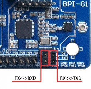
WIFI (CC3200), BLE (CC2540 / 1) and ZIGBEE (CC2530) are interconnected through STM32F103CB serial port, they can work alone, can also coordinate the work will be given below communication connections between the modules schematic.5.1 CC3200 connection with F103.
5.2 CC2540 connection with F103
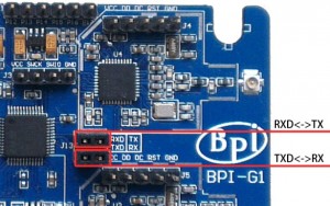
5.3 CC2530 connection with F103
6. Status LEDs for each module
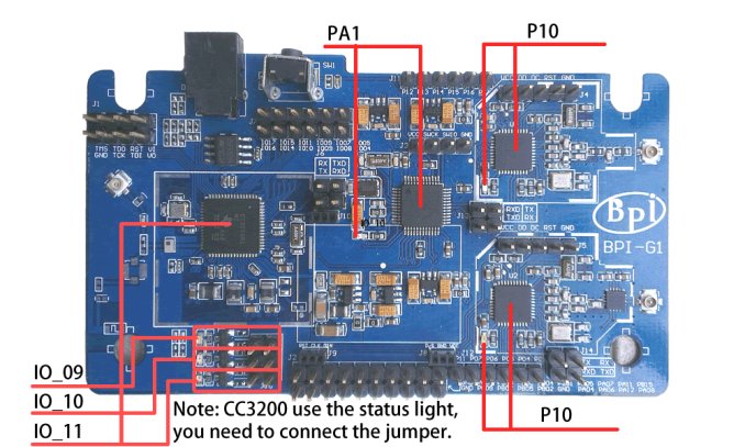
In each module has its own status indicators, in addition there are three status lights CC3200, the others were all one, and these status lights are controlled by the GPIO module.
7. TI CC3200 mode selection jumper
7.1 Programming mode
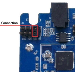
Under the programming mode, you need to VI and VO short on power, CC3200 will receive as a writer, it will be the serial data received by the SPI mode file system writes to the external SFLASH, but the programming is completed after not running, you need to disconnect VI and VO, then on again, then it will be read in the file system SFLASH into memory and execute code. As shown in Figure.
7.2 Run mode
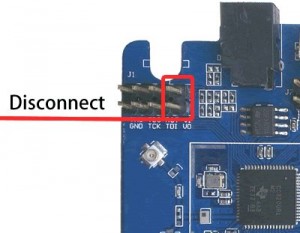
Run mode, you need to disconnect VI and VO, then power on, CC3200 will SFLASH read from the file system into memory and run. In this mode, plug in the JTAG interface, using the IDE’s DEBUG function, and the code will be downloaded from the JTAG interface to the memory to run, you can perform single-step debugging. For fast functional verification, this is the fastest way. However, after a reset circuit, CC3200 will be new to SFLASH read the file system operation. As shown in Figure.
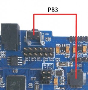
8. Button
BPI G1 has a button, which is connected to the PB3 pin F103, in the middle of a pullup resistor in parallel, when the key is pressed, the pin will be low-level information. Figure.